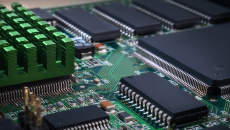
In the realm of modern technology, where sleekness and efficiency reign supreme, the art and science of miniaturization play a pivotal role. At the heart of this phenomenon lies the intricate world of Integrated Circuit (IC) chips. These diminutive marvels power our digital age, enabling everything from smartphones and laptops to spacecraft and medical devices. In this exploration, we delve into the fascinating landscape of IC chips, uncovering the secrets behind their design, functionality, and significance in shaping our interconnected world.
Understanding Integrated Circuits
Integrated circuits, often referred to as microchips or simply ICCHIPS, are tiny electronic components packed with thousands to billions of transistors, resistors, and capacitors. These components are etched onto a semiconductor material, typically silicon, through a process known as photolithography. The integration of these elements onto a single chip drastically reduces size, enhances performance, and lowers production costs compared to discrete electronic components.
Components of IC Chips:
- Transistors: These semiconductor devices serve as the fundamental building blocks of ICs, amplifying or switching electronic signals.
- Resistors: Resistors regulate the flow of electric current within the circuit, controlling voltage and current levels.
- Capacitors: Capacitors store and release electrical energy, stabilizing voltage and filtering noise within the circuit.
The Evolution of Miniaturization
The journey of miniaturization traces back to the mid-20th century when engineers and scientists envisioned compact electronic systems with increased reliability and efficiency. The pioneering work of figures like Jack Kilby and Robert Noyce in the late 1950s paved the way for the development of the first integrated circuits. Initially, these early ICs contained only a handful of transistors, but with advancements in fabrication techniques and design methodologies, the complexity of ICs grew exponentially.
Milestones in Miniaturization:
- Moore’s Law: Coined by Gordon Moore, the co-founder of Intel, Moore’s Law observes that the number of transistors on an IC doubles approximately every two years, driving the relentless march towards smaller and more powerful chips.
- Shrinking Die Sizes: Technological breakthroughs in photolithography and semiconductor manufacturing have enabled the production of ICs with increasingly smaller feature sizes, measured in nanometers.
- System-on-Chip (SoC) Integration: SoC integration consolidates multiple functions onto a single chip, incorporating microprocessors, memory, and peripherals within a compact footprint.
The Anatomy of IC Fabrication
The fabrication of IC chips is a meticulously orchestrated process involving numerous sequential steps performed in cleanroom environments. Each stage of fabrication contributes to the precise formation of transistor gates, interconnects, and circuit elements on the semiconductor substrate.
Key Stages in IC Fabrication:
- Substrate Preparation: The semiconductor substrate, typically a silicon wafer, undergoes rigorous cleaning and preparation to ensure a pristine surface for subsequent processing.
- Deposition: Thin layers of materials such as silicon dioxide and polysilicon are deposited onto the wafer using techniques like chemical vapor deposition (CVD) or physical vapor deposition (PVD).
- Photolithography: A photosensitive layer, called photoresist, is applied to the wafer and patterned using ultraviolet light and photomasks to define the circuit features.
- Etching: Exposed regions of the wafer are selectively etched away using plasma or chemical solutions, leaving behind the desired circuit patterns.
- Doping: Dopant atoms, such as phosphorus or boron, are introduced into the semiconductor to modify its electrical properties and create regions of positive (p-type) and negative (n-type) conductivity.
- Metallization: Metal layers, typically aluminum or copper, are deposited onto the wafer to form interconnects that link various components of the circuit.
Applications and Impact
The pervasive influence of integrated circuit distributor extends across virtually every sector of modern society, revolutionizing communication, computing, healthcare, transportation, and beyond. From the microprocessors powering our smartphones to the control systems guiding autonomous vehicles, ICs serve as the bedrock of technological innovation and progress.
Diverse Applications of IC Chips:
- Consumer Electronics: Smartphones, tablets, laptops, and wearables rely on ICs for processing, memory storage, and wireless connectivity.
- Industrial Automation: ICs enable precision control and monitoring in manufacturing processes, robotics, and industrial machinery.
- Healthcare: Medical devices, imaging systems, and diagnostic equipment leverage ICs for data acquisition, signal processing, and patient monitoring.
- Aerospace and Defense: ICs power avionics, navigation systems, and radar technology in commercial aircraft, satellites, and military platforms.
Challenges and Future Trends
While the miniaturization of ICs has propelled technological advancement to unprecedented heights, it also presents formidable challenges in terms of thermal management, power consumption, and manufacturing complexity. As the industry continues to push the boundaries of semiconductor scaling, researchers and engineers are exploring novel materials, device architectures, and integration techniques to sustain the momentum of innovation.
Emerging Trends in IC Design:
- Beyond Moore’s Law: Innovations such as three-dimensional (3D) integration, quantum computing, and neuromorphic computing offer promising avenues for circumventing the limitations of traditional scaling.
- Heterogeneous Integration: Combining disparate technologies, such as silicon CMOS, gallium nitride (GaN), and silicon carbide (SiC), enables the development of specialized ICs tailored to specific applications.
- Energy-Efficient Design: Techniques such as voltage scaling, dynamic power management, and low-power circuit design are essential for mitigating the energy consumption of ICs in portable devices and IoT endpoints.
Conclusion
In conclusion, the art and science of miniaturization encapsulate the ingenuity, precision, and innovation driving the evolution of integrated circuit technology. From the humble beginnings of early transistor-based circuits to the cutting-edge advancements of today, IC chips continue to reshape our world, enabling new possibilities and pushing the boundaries of what is technologically achievable. As we navigate the complexities of an increasingly interconnected digital landscape, the journey of miniaturization remains a testament to the boundless creativity and vision of humanity.


